Application guide by addaScanCompare the inspection task, imaging conditions and validation steps with your own production line.
- Task
- PCBA solder inspection with 3D height
- Decision focus
- Dimensional measurement
- Workflow
- Select the joint map and recipe.
- Validation
- Good joints across normal board warp
Solder height, bridges and missing depth evidence
Original explanatory diagrams show the product states and inspection questions. They are schematics, not captured inspection results.
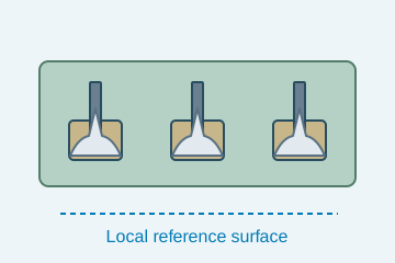
Relative height is evaluated against a local base.
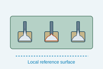
A low profile needs the agreed geometric rule.
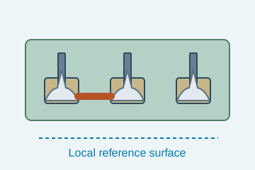
Connected material between features is a separate fault.
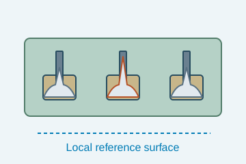
An excessive local peak changes the profile.
Select an image to view it at full size.
Establish the local board surface before measuring a solder joint
Explore Dimensional measurement and Assembly verification to connect this inspection task with the wider station requirements.
Swipe across the table to compare all columns →
| Decision | Evidence to use | Rule to agree |
|---|---|---|
| Reference valid | Locate the board and local base surface. | Account for board warp. |
| Joint geometry acceptable | Evaluate the required relative height and shape. | Use fault-specific criteria. |
| Depth coverage complete | Check valid data at every required feature. | Hold incomplete or shadowed regions. |
Use fault-specific geometry rather than one height threshold
Fit a suitable local reference outside the solder and components. Evaluate the required relative height or shape within each joint region, excluding invalid points without inventing a surface across large gaps. A low-solder rule, a bridge between adjacent regions and a sharp peak require different geometric evidence.
2D imaging can support visible presence, location and appearance. 3D adds observable height and shape; electrical testing addresses function. Combining these methods is useful when their responsibilities are explicit. A bright reflective void in a depth map is not automatically a depression, and a good solder profile does not prove electrical continuity.
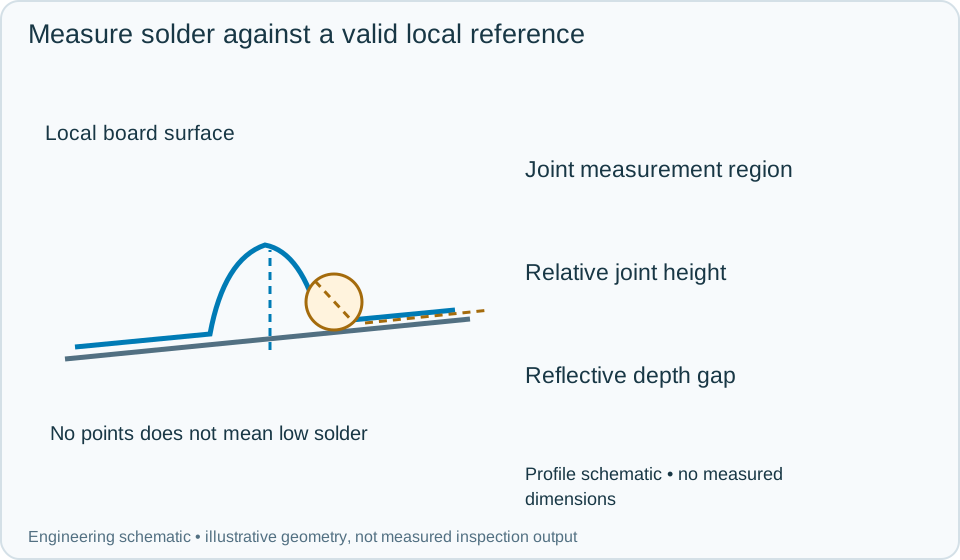
On a small screen, scroll across the diagram to inspect the labels.
Swipe across the table to compare all columns →
| Approach | Useful when | What to validate |
|---|---|---|
| 2D inspection | Visible presence and appearance answer the requirement. | It does not directly add height. |
| 3D line profiling | Relative height or surface shape is needed. | Validate reflection, scanning and reference extraction. |
| Combined inspection and electrical test | Geometry and function both require acceptance. | Assign each requirement to its own evidence. |
Worked example: a reflective joint appears to have low solder
In an illustrative scan, the joint centre contains missing depth returns. A naive average of the remaining points would produce a low value. The valid-data test instead marks the required region incomplete. Reacquire from the qualified scan arrangement or route the board to another approved check.
A second joint has complete valid data and genuinely low relative geometry, so it fails the defined shape rule. A third has connected material between neighbouring joint regions and fails the bridge rule independently. Keep these outcomes at joint level under the board identity. Do not release the board because most joints passed while an obscured joint remains unresolved. After rework, repeat the affected checks and preserve both attempts and the final board disposition.
Swipe across the table to compare all columns →
| Observed evidence | Inspection decision | Action and retained record |
|---|---|---|
| A joint's reflective centre has missing depth data while surrounding points are low. | Required geometry is unmeasured; low solder cannot be inferred. | Keep the valid-data mask, local reference and joint ID. Reacquire or use the approved alternative check before completing the board result. |
| Valid relative geometry falls below the agreed solder-shape requirement. | Joint geometry fails within the qualified measurement scope. | Retain the measured region and board identity, route for rework or rejection and preserve the failed result when recording the new attempt. |
| Connected material spans two adjacent joint regions despite acceptable individual peaks. | Bridge criterion fails independently of peak height. | Store the connected region and neighbouring joint IDs, hold the board and retain separate functional-test responsibilities after repair. |
When should uncertain solder-height data be held?
- 01Identify and locate the boardSelect the joint map and recipe.
- 02Acquire the depth profileScan every required exposed feature.
- 03Reference and evaluateMeasure relative geometry using valid data.
- 04Record by jointKeep fault location and board disposition together.
Locate the board and join the geometry results to its identity and inspection recipe. A reflective or shadowed region may produce incomplete depth data rather than a trustworthy low-height result. Record that condition explicitly. If the scan requires multiple passes, confirm that all required joints are covered before releasing the board.
Validate local referencing across normal board warp
Use known acceptable and faulty joints, permitted board warp, reflective surfaces and tall components that create shadows. Check the local reference against an appropriate independent measurement where dimensions are specified.
Retain the joint map, reference region, valid-data mask and selected geometric results. This allows a false alarm to be traced to reference fitting, coverage or actual solder shape instead of treating every low numeric output as the same defect.
Swipe across the table to compare all columns →
| Challenge | What the trial should establish |
|---|---|
| Good joints across normal board warp | Test the local reference method. |
| Low solder, bridges and peaks | Confirm independent geometric decisions. |
| Glossy joints beside tall components | Check valid data and shadow coverage. |
| Wrong board recipe or incomplete scan | Verify hold and traceability behaviour. |
What 3D solder-height inspection cannot establish
Exposed solder geometry is not proof of electrical continuity, hidden-joint integrity or component function. Highly reflective surfaces, tall neighbouring components and inaccessible joints can restrict coverage. Do not infer full-board coplanarity or every pin requirement from a solder-height application.
Use Vision measurement vs CMM and gauges to develop the related acceptance and integration questions for your trial.
Board variants and height references to provide
Provide board families, target joints, known solder faults, accepted geometric variation, reference measurements where relevant and the available scan path around tall components.
Use the optical and recovery challenges above when applying the architecture choices in HIKROBOT and other vision solutions comparison.
Scope and budget
The vision system cost guide explains general 3D measurement and integration cost factors; board-specific coverage and validation require their own scope.
Testing and handover
Use the testing and handover process to agree reference planes, occluded features and uncertain measurements, separately from electrical or full-board AOI testing.